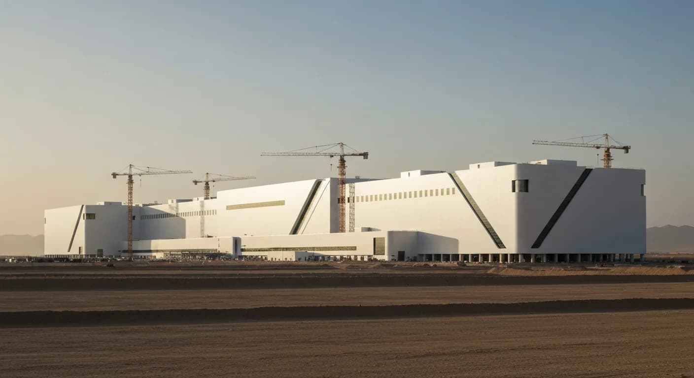
Elon Musk confirmed on March 14 that Tesla's Terafab project — the company's audacious entry into semiconductor manufacturing — will officially launch on March 21. The $25 billion facility represents the most ambitious vertical integration play in the AI hardware industry, combining logic processing, memory storage, and advanced chip packaging under a single roof.
No private company outside of TSMC and Samsung currently operates at this scale.
What Terafab Will Build
The facility is designed to produce Tesla's fifth-generation AI chip, the AI5, using 2-nanometer process technology — the most advanced node currently in commercial production. Production targets call for 100,000 wafer starts per month, with output projected between 100 and 200 billion custom AI and memory chips per year once the facility reaches full capacity.
The AI5 chip will power three of Tesla's most critical product lines: the Full Self-Driving software stack, the Cybercab robotaxi program, and the Optimus humanoid robot. Each of these products requires massive onboard compute, and Musk has repeatedly warned investors that relying on external foundries would create a supply bottleneck within three to four years.
Why Tesla Is Building Its Own Fab
The decision to build in-house reflects a broader trend among major tech companies seeking to reduce dependence on a concentrated semiconductor supply chain. Apple, Google, and Amazon have all designed custom silicon, but they still rely on TSMC for fabrication. Tesla is attempting to own the entire pipeline from chip design through manufacturing.
Musk's rationale is partly strategic and partly mathematical. Tesla projects that its fleet of autonomous vehicles and robots will require orders of magnitude more AI inference chips than any foundry partner can guarantee on Tesla's timeline. By controlling fabrication, the company avoids competing with hyperscalers for limited foundry capacity.
The Scale of the Bet
At $25 billion, Terafab is one of the most expensive private infrastructure projects in American history. For context, TSMC's Arizona fab complex — backed by $6.6 billion in federal CHIPS Act subsidies — represents a total investment of over $65 billion across three planned fabs. Tesla is attempting a comparable facility with no announced government subsidies.
Analysts are divided on whether Tesla can execute. Semiconductor fabrication at the 2nm node requires extreme precision, deep institutional knowledge, and years of yield optimization. Companies that have attempted to build fabs from scratch — notably Intel's foundry efforts — have faced persistent delays and cost overruns.
Market Implications
Tesla shares declined 0.96% following the announcement, with some investors expressing caution about the project's capital requirements. If successful, Terafab would give Tesla a structural cost advantage in AI inference hardware and reduce its vulnerability to geopolitical disruptions in the chip supply chain.
The launch on March 21 will likely involve the formal groundbreaking and initial equipment installation rather than chip production. Small-batch AI5 production is expected later in 2026, with volume manufacturing projected for 2027.
For the broader AI industry, Terafab raises a fundamental question: will the next era of AI be defined not by who builds the best models, but by who controls the silicon they run on?